Integrated Circuit
Substrates (ICS)

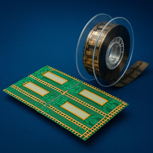
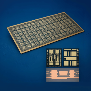
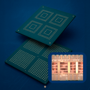
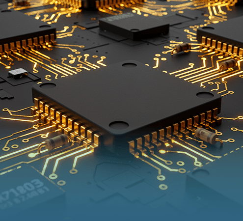
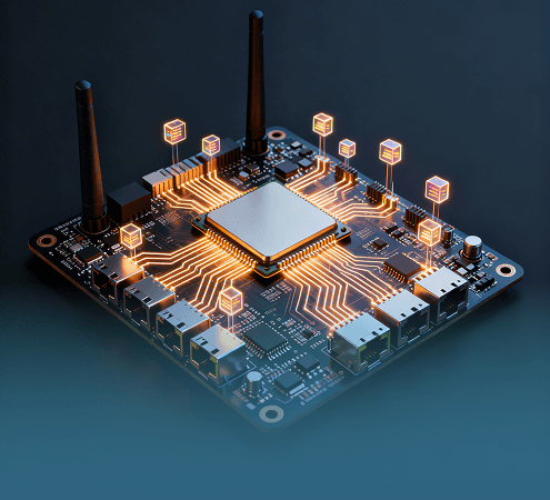
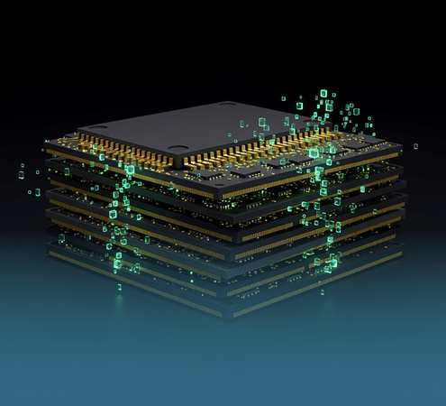
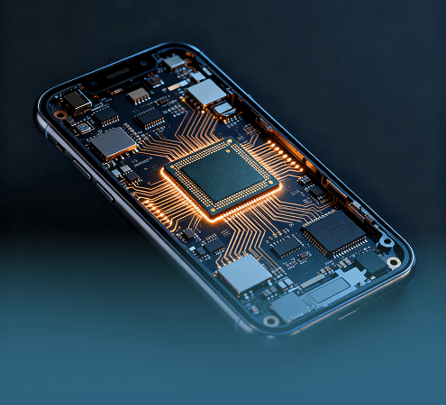
Integrated Circuit Substrates (ICS) are high-precision interconnection platforms that serve as the bridge
between semiconductor chips and printed circuit boards, enabling efficient electrical routing, power
distribution, and thermal management. Built with ultra-fine circuitry and advanced substrate materials, ICS
provide the foundation for high-performance semiconductor packaging in compact electronic systems.

Sputtered-Core Substrate
Coreless ABF
Substrate
FCBGA ABF
Substrate
Advanced Packaging Substrate
What We Provide
  • Integrating advanced SAP, HDI, and coreless platform technologies for high-density circuit designs for next-generation products
  • IC Substrates for Advanced Packaging Applications, such as:
    • Sputtered-core substrate for Au Au TCB, TAB & Cu Pillar FC
    • ABF based Coreless Substrates for SiP & MCM, used in PMIC applications for GaN & RF/TVS/PA applications for mobile devices. Up to 3.5 layers with wettable flank, max unit size 10x10mm with thickness of 200um, embedded traces min line/space 20/20um with 20um copper thickness
    • ABF based FCBGA substrates for High IO Count FC Dies, in Processor Applications. Up to 10 layers (4+2+4) with ALIC using copper filled vias & SOP + Coining on die side
    • Advanced Packaging Substrates: Electroformed (Mushroom, Overhang) Substrates for extremely thin LF packages, on removal carrier
  • Finishing: OSP, AT, NiAu, NiPdAu, ENIG, ENEPIG
Competitive Advantages
  • Shrink package size by layer thickness trimming using grinding & line space scaling by SAP
  • SAP processing on ABF to enable fine line features & integrated formation of cu filled vias with trace
  • Any shape pure copper photo vias to provide best vertical thermal performance
  • Front-to-end reel-to-reel format manufacturing & delivery, featuring ultra-fine line circuitry using SAP process.
    Key process enablers image stitching, gapless coverlay lamination, zipping, wet chemical PI etching, direct Au plating (without Ni barrier), delivery in multiple tape formats after 100% back-end testing

Applications

ASIC (Application-Specific Integrated Circuits)
PMIC (Power
Management IC)
MEMS (Micro Electro Mechanical Sensor)
Image processing
chips (ISP)
Server and data
center semiconductors
Networking and
communication chips
Memory chips
(DRAM / NAND)
Mobile application
processors
From concept to production,
our engineering team partners closely
with customers to deliver
optimal performance, manufacturability,
and value across a wide range of applications.