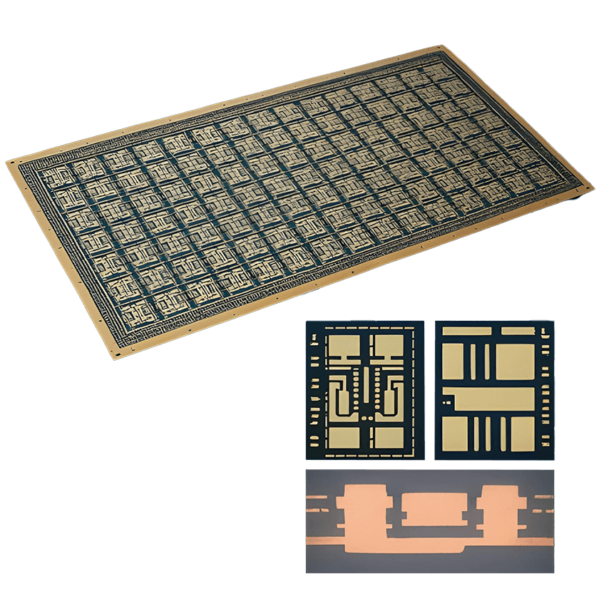
Advancing
Interconnect
Solutions for
Modern Electronics
Additively Formed
Interconnects (AFI)
The demand for modern electronics continues to rise – components need to provide more
functions in lesser space. SQAI addresses this industry requirement
by offering Additively Formed Interconnects (AFI) with Semi-Additive Process (SAP).
These technologies are crucial for applications requiring extreme miniaturization, such as
IC substrates and smartphones.
Semi-Additive Process (SAP)
SAP uses a non-conductive substrate with an extremely thin copper layer (less than 2 μm) plated onto it.
Copper is then built up only in the open areas defined by a precise photoresist pattern to form the desired structure. After stripping the photoresist, the very thin copper layer remaining between the tracks is etched away using flash etching, leaving the desired copper pattern.
The traces have nearly perfect rectangular cross-sections with sharp and defined edges. SAP offers the best control over dimensions and trace geometry.
line and space down to 10 micrometers and below.
These technologies are crucial for applications requiring extreme miniaturization, such as IC substrates and AI semiconductors. This advanced technology enables ultra-fine circuit structures, aligned with future scaling roadmap of electronics world.
The precise shape of conductors from AFI technologies ensure the undistorted high-frequency signals necessary for advanced telecommunications. SAP technology excels in line and space width ranging from 75 to 10 micrometers.
Explore Our
Capabilities (ICS)
Capabilities (ICS)
Electronic Innovation